Computer organization and architecture miscellaneous
- Suppose the functions F and G can be computed in 5 and 3 nanoseconds by functional units UF and UG, respectively. Given two instances of UF and two instances of UG, it is required to implement the computation F(G(Xi)) for 1 ≤ i ≤ 10. Ignoring all other delays, the minimum time required to complete this computation is _______ nanoseconds.
-
View Hint View Answer Discuss in Forum
This concept is used in pipelining. The important thing here is UF as it takes 5 ns while UG takes 3 ns only. One have to do 10 such calculations. According to question, we have 2 instances of UF and UG respectively. So, UF can be done in 50 / 2 = 25 nano seconds. For the start, UF needs to wait for UG output for 3 ns and rest all are pipelined and hence no more wait. Therefore, the answer will be :
3 + 25 = 28 nsCorrect Option: A
This concept is used in pipelining. The important thing here is UF as it takes 5 ns while UG takes 3 ns only. One have to do 10 such calculations. According to question, we have 2 instances of UF and UG respectively. So, UF can be done in 50 / 2 = 25 nano seconds. For the start, UF needs to wait for UG output for 3 ns and rest all are pipelined and hence no more wait. Therefore, the answer will be :
3 + 25 = 28 ns
- The stage delays in a 4-stage pipeline are 800, 500, 400 and 300 picoseconds. The first stage (with delay 800 picoseconds) is replaced with a functionally equivalent design involving two stages with respective delays 600 and 350 picoseconds. The throughput increase of the pipeline is __________ percent.
-
View Hint View Answer Discuss in Forum
Old design tp = 800
New design tp = 600Throughput = 800 - 600 × 100% = 33.33% 600 Correct Option: C
Old design tp = 800
New design tp = 600Throughput = 800 - 600 × 100% = 33.33% 600
- Instruction execution in a processor is divided into 5 stages. Instruction Fetch (IF). Instruction Decode (ID). Operand Fetch (OF). Execute (EX), and Write Back (WB). These stages take 5, 4, 20, 10, and 3 nanoseconds (us) respectively. A pipelined implementation of the processor requires buffering between each pair of consecutive stages with a delay of 2 ns. Two pipelined implementations of the processor are contemplated :
(i) a naive pipeline implementation (NP) with 5 stages and
(ii) an efficient pipeline (EP) where the OF stage is divided into stages OF1 and OF2 with execution times of 12 ns and 8 ns respectively. The speedup (correct to two decimal places) achieved by EP over NP in executing 20 independent instructions with no hazards is _______ .
-
View Hint View Answer Discuss in Forum
Given for Native pipeline, the number of stages (k) = 5.
tP1 = Max(Stage delay + buffer delay)
Buffer delay = 2nS
Stage delay = 5, 4, 20, 10, 3
So
tP1 = Max((5 + 2), (4 + 2), (20 + 2), (10 + 2), (3 + 2))
= Max (7, 6, 22, 12, 5)
Maximum value is 22.tP1
Number of instruction (n) = 20
So, execution time for native pipeline (NP).
Then,
Execution time (TNP) = (k + n – 1) tP1
= (5 + 20 – 1) 22 n sec.
TNP = 528 n sec.
Now, for efficient pipeline (TEP), the number. of stages (k = 6), n = 20, tP2 = ? tP2 = Max (Stage delay + Buffer delay)
= (12 nS + 2 nS) = 14 ns.
So, TEP = (k + n – 1) tP2
= (6 + 20 – 1) * 14 = 350 n sec.Speed up (S) = TNP = 528 = 1.508 TEP 350 Correct Option: B
Given for Native pipeline, the number of stages (k) = 5.
tP1 = Max(Stage delay + buffer delay)
Buffer delay = 2nS
Stage delay = 5, 4, 20, 10, 3
So
tP1 = Max((5 + 2), (4 + 2), (20 + 2), (10 + 2), (3 + 2))
= Max (7, 6, 22, 12, 5)
Maximum value is 22.tP1
Number of instruction (n) = 20
So, execution time for native pipeline (NP).
Then,
Execution time (TNP) = (k + n – 1) tP1
= (5 + 20 – 1) 22 n sec.
TNP = 528 n sec.
Now, for efficient pipeline (TEP), the number. of stages (k = 6), n = 20, tP2 = ? tP2 = Max (Stage delay + Buffer delay)
= (12 nS + 2 nS) = 14 ns.
So, TEP = (k + n – 1) tP2
= (6 + 20 – 1) * 14 = 350 n sec.Speed up (S) = TNP = 528 = 1.508 TEP 350
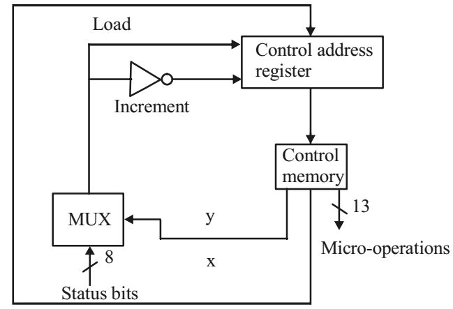
- The micro-instructions stored in the control memory of a processor have a width of 26 bit. Each micro-instruction is divided into three fields; a micro-operation field of 13 bit, a next address field (X), and a MUX select field (Y), there are 8 status bits in the inputs of the MUX.

How many bits are there in the X and Y fields, and what in the size of the control memory in number of words?
-
View Hint View Answer Discuss in Forum
MUX has 8 states bits as input lines so we require 3 select inputs to select & input lines. No. of bits in control memory next address field = 26 – 13 – 3
= 10
10 bit addressing, we have 210 memory size. So X, Y size = 10,3,1024
Hence (a) is correct option.Correct Option: A
MUX has 8 states bits as input lines so we require 3 select inputs to select & input lines. No. of bits in control memory next address field = 26 – 13 – 3
= 10
10 bit addressing, we have 210 memory size. So X, Y size = 10,3,1024
Hence (a) is correct option.
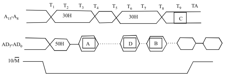
- Consider the 8085 instruction IN 09H stored as follows:

Add the following incomplete timing diagram for the instruction :
(a) Write the contents of the boxes, A, B, C and D in hexademcimal in your answer sheet do not draw any pictures.
(b) Write the state of both ALE and RD pins at times T1, T2, T3 and T4. (c) How do you generate the signal that tells the peripheral to put the data on the bus? Answer by completing the following statement in your answer book : By combining signals ..............
-
View Hint View Answer Discuss in Forum
(a) A : D A H B : 0 9 H
C : 0 9 H D : 5 1 H
(b) ALE : T1 = 1
T2 = T3 = T4 = 0
RD : T1 = 1
T2 = T3 = 0. T4 = 1
(c) The IO/ M signal and RD signalCorrect Option: D
(a) A : D A H B : 0 9 H
C : 0 9 H D : 5 1 H
(b) ALE : T1 = 1
T2 = T3 = T4 = 0
RD : T1 = 1
T2 = T3 = 0. T4 = 1
(c) The IO/ M signal and RD signal

