Physical electronics devices and ics miscellaneous
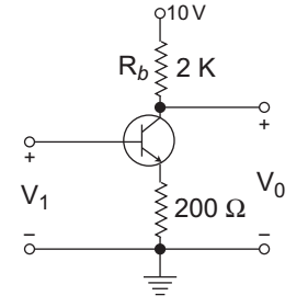
- In the circuit shown below V1 = 2·7 V, VBE = 0·7 V and β >> 1. The gm of the transistor is—
-
View Hint View Answer Discuss in Forum
The given circuit (i.e., fig)
Given, V1 = 2·7 V, VBE = 0·7 V and β >> 1 means IB ≈ OA
Applying KVL to the input section, we get
V1 – VBE – IC · 200 = 0
or 2·7 – 0·7 – IC · 200 = 0or IC = 2 A 200 Now, gm = IC = 2/200 A = 400 mA/ V VT 25 mV
or gm = 400 m mho
Hence alternative (B) is the correct choice.
Correct Option: B
The given circuit (i.e., fig)
Given, V1 = 2·7 V, VBE = 0·7 V and β >> 1 means IB ≈ OA
Applying KVL to the input section, we get
V1 – VBE – IC · 200 = 0
or 2·7 – 0·7 – IC · 200 = 0or IC = 2 A 200 Now, gm = IC = 2/200 A = 400 mA/ V VT 25 mV
or gm = 400 m mho
Hence alternative (B) is the correct choice.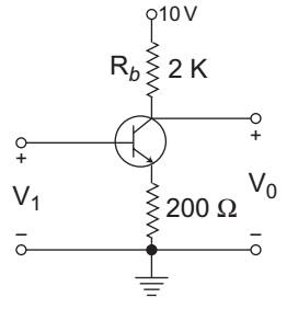
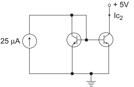
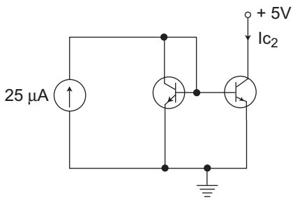
- The two transistors in figure are identical. If β = 25, the current Ic2 is—
-
View Hint View Answer Discuss in Forum
The given figure (i.e., fig)
From figure Iref = 25 µA
Since both the transisors are identical
Therefore IB1 = IB2 = IB & VBE1 = VBE2 = VBE
Now, Iref = IB1 + IC1 + IB2 = IB + βIB + IB = (β + 2) IBand IC2 = βIB2 = BIB1 = βIB = β·Iref (β + 2) or IC2 = 25· 25 µA = 23·2 µA (25 + 2)
Hence alternative (B) is the correct choice.

Correct Option: B
The given figure (i.e., fig)
From figure Iref = 25 µA
Since both the transisors are identical
Therefore IB1 = IB2 = IB & VBE1 = VBE2 = VBE
Now, Iref = IB1 + IC1 + IB2 = IB + βIB + IB = (β + 2) IBand IC2 = βIB2 = BIB1 = βIB = β·Iref (β + 2) or IC2 = 25· 25 µA = 23·2 µA (25 + 2)
Hence alternative (B) is the correct choice.
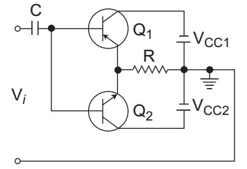
- In the circuit shown below during the negative cycle, the input signal—
-
View Hint View Answer Discuss in Forum
The given circuit (i.e., fig)
From given circuit, we observe that transistor Q1 is pnp type while Q2 is npn type. So, during the negative cycle of the input signal, transistor Q1 will conduct while Q2 will not conduct i.e., Q2 is cut-off mode. Hence alternative (B) is the correct choice.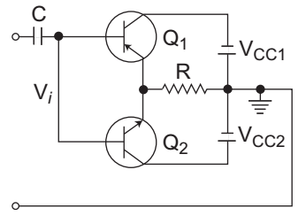
Correct Option: B
The given circuit (i.e., fig)
From given circuit, we observe that transistor Q1 is pnp type while Q2 is npn type. So, during the negative cycle of the input signal, transistor Q1 will conduct while Q2 will not conduct i.e., Q2 is cut-off mode. Hence alternative (B) is the correct choice.
- Match List-I (Devices) with List-II (Characteristic) and select the correct answer using the code given below the lists:
List-I
(a) BJT
(b) MOSFET
(c) Tunnel diode
(d) Zener diode
List-II
1. Voltage controlled negative resistance
2. High current gain
3. Voltage regulation
4. High input impedance Codes:
-
View Hint View Answer Discuss in Forum
● BJT → High current gain
● MOSFET → High input impedance
● Tunnel diode → Voltage controlled negative resistance
● Zener diode → Voltage regulationCorrect Option: C
● BJT → High current gain
● MOSFET → High input impedance
● Tunnel diode → Voltage controlled negative resistance
● Zener diode → Voltage regulation
- The fT of a BJT is related to its gm, Cπ and Cµ as—
-
View Hint View Answer Discuss in Forum
The unity-gain bandwidth frequency of a BJT is related to its gm, Cπ and Cµ by relation
fT = gm 2 (Cπ + Cµ) Correct Option: C
The unity-gain bandwidth frequency of a BJT is related to its gm, Cπ and Cµ by relation
fT = gm 2 (Cπ + Cµ)

