Physical electronics devices and ics miscellaneous
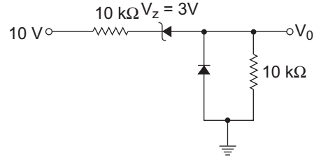
- Assuming the forward diode drop as 0V, the output voltage V0, as shown in figure—
-
View Hint View Answer Discuss in Forum
The given figure
The above figure can be redrawn as
from above figure
10 – 10 K.I. – 3 – 10 K.I. = 0or I = 7 = 7 mA 20 K 20 and V0 = 10 K.I. = 10 K. 7 mA = 3·5 V 20
Hence alternative (C) is the correct choice.Correct Option: C
The given figure
The above figure can be redrawn as
from above figure
10 – 10 K.I. – 3 – 10 K.I. = 0or I = 7 = 7 mA 20 K 20 and V0 = 10 K.I. = 10 K. 7 mA = 3·5 V 20
Hence alternative (C) is the correct choice.
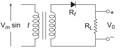
- Consider the circuit given below where Rf is the diode forward resistance and RL the load resistance. What is the average rectified current equal to?
-
View Hint View Answer Discuss in Forum
The given circuit
The above circuit is half wave rectifier. ThereforeVar = Vm π Iar = Im = Vm π (RL + Rf)
Hence alternative (B) is the correct choice.Correct Option: B
The given circuit
The above circuit is half wave rectifier. ThereforeVar = Vm π Iar = Im = Vm π (RL + Rf)
Hence alternative (B) is the correct choice.
- A p-n junction has a built-in potential of 0·8 V. The depletion layer width at a reverse bias of 1·2 V is 2 µm. For a reverse bias of 7·2 V, the depletion layer width will be—
-
View Hint View Answer Discuss in Forum
We know that depletion layer width and reverse bias voltage are related by expression
d α 
1 + Vr 
1 / 2 VB
Where,
d = depletion
width Vr = applied reverse bias voltage
VB = built in potentialNow, d1 = VB + VR1 d2 VB + VR2 or d2 = VB + VR2 1 / 2 × d1 VB + VR1 or d2 = 0·8 + 7·2 1 / 2 × µm 0·8 + 1·2 or d2 = 8 1 / 2 × 2µm = 4µm 2
Hence alternative (A) is the correct choice.
Correct Option: A
We know that depletion layer width and reverse bias voltage are related by expression
d α 1 + Vr 1 / 2 VB
Where,
d = depletion
width Vr = applied reverse bias voltage
VB = built in potentialNow, d1 = VB + VR1 d2 VB + VR2 or d2 = VB + VR2 1 / 2 × d1 VB + VR1 or d2 = 0·8 + 7·2 1 / 2 × µm 0·8 + 1·2 or d2 = 8 1 / 2 × 2µm = 4µm 2
Hence alternative (A) is the correct choice.
- Which of the following is not associated with a pn junction?
-
View Hint View Answer Discuss in Forum
Channel length modulation is not associated with pn-junction diode.
Correct Option: D
Channel length modulation is not associated with pn-junction diode.
- The softness factor for soft-recovery and fast-recovery diodes are respectively—
-
View Hint View Answer Discuss in Forum
Softness factor for soft recovery diodes are 1 and for fast recovery diodes are < 1.
Correct Option: D
Softness factor for soft recovery diodes are 1 and for fast recovery diodes are < 1.

