Semiconductor Electronics : Materials, Devices and Simple Circuits
- A semi-conducting device is connected in a series circuit with a battery and a resistance. A current is found to pass through the circuit. If the polarity of the battery is reversed, the current drops to almost zero. The device may be
-
View Hint View Answer Discuss in Forum
In reverse bias, the current through a p-n junction is almost zero.
Correct Option: A
In reverse bias, the current through a p-n junction is almost zero.
- Which of the following when added acts as an impurity into silicon produced n-type semi-conductor?
-
View Hint View Answer Discuss in Forum
n-type of silicon semiconductor is formed when impurity is mixed with pentavalent atom. Out of given choices only phosphorus is pentavalent.
Correct Option: A
n-type of silicon semiconductor is formed when impurity is mixed with pentavalent atom. Out of given choices only phosphorus is pentavalent.
- In a junction diode, the holes are due to
-
View Hint View Answer Discuss in Forum
Holes are produced due to missing of electrons.
Correct Option: D
Holes are produced due to missing of electrons.
- Application of a forward bias to a p–n junction
-
View Hint View Answer Discuss in Forum

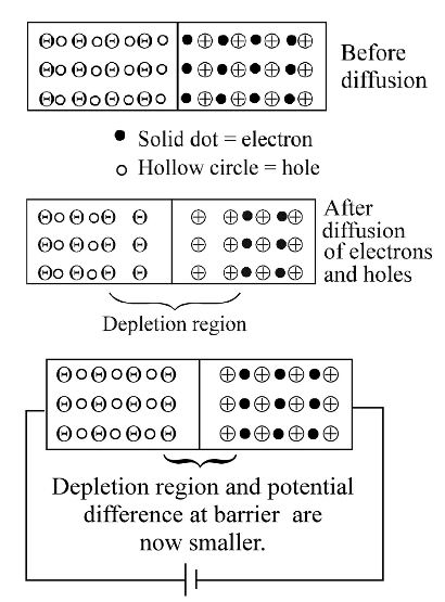
Number of donors is more because electrons from –ve terminal of the cell pushes (enters) the n side and decreases the number of uncompensated pentavalent ion due to which potential barrier is reduced. The neutralised pentavalent atom are again in position to donate electrons.Correct Option: C

Number of donors is more because electrons from –ve terminal of the cell pushes (enters) the n side and decreases the number of uncompensated pentavalent ion due to which potential barrier is reduced. The neutralised pentavalent atom are again in position to donate electrons.
- The cause of the potential barrier in a p-n diode is
-
View Hint View Answer Discuss in Forum
During the formation of a junction diode, holes from p-region diffuse into n-region and electrons from n-region diffuse into p-region. In both cases, when an electron meets a hole, they cancel the effect of each other and as a result, a thin layer at the junction becomes free from any of charge carriers. This is called depletion layer. There is a potential gradient in the depletion layer, negative on the p-side and positive on the n-side. The potential difference thus developed across the junction is called potential barrier.
Correct Option: D
During the formation of a junction diode, holes from p-region diffuse into n-region and electrons from n-region diffuse into p-region. In both cases, when an electron meets a hole, they cancel the effect of each other and as a result, a thin layer at the junction becomes free from any of charge carriers. This is called depletion layer. There is a potential gradient in the depletion layer, negative on the p-side and positive on the n-side. The potential difference thus developed across the junction is called potential barrier.

