Analog circuits miscellaneous
- For the circuit of the given figure with an ideal operational amplifier, maximum phase shift of the output Vout with reference to the input Vin is
-
View Hint View Answer Discuss in Forum
From the circuit,
V+ = Vin 1 + jωRC
and V– =V+ (Ideal OPAMP) NowNow Vin - V– = V– – V0 R1 R1
⇒ V0 = 2V– – Vin = 2V+ – Vin= 
2 - 1 
Vin = 1 - jωRC V0 1 + jωRC 1 + jωRC
∴ ∠ (V0 / Vi) = - 2 tan-1 ωRC
For – 90 ≤ θ ≤ 90°
Phase-shift ∠ (V0 / Vi) = ± 180°
Correct Option: D
From the circuit,
V+ = Vin 1 + jωRC
and V– =V+ (Ideal OPAMP) NowNow Vin - V– = V– – V0 R1 R1
⇒ V0 = 2V– – Vin = 2V+ – Vin= 2 - 1 Vin = 1 - jωRC V0 1 + jωRC 1 + jωRC
∴ ∠ (V0 / Vi) = - 2 tan-1 ωRC
For – 90 ≤ θ ≤ 90°
Phase-shift ∠ (V0 / Vi) = ± 180°
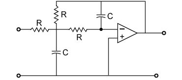
- The transfer function of a second order LP filter shown in the given figure is
-
View Hint View Answer Discuss in Forum
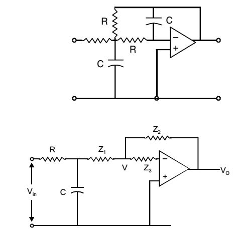
Using ∆ – Y conversion,Z1 = R2Cs 2RCs + 1 Z2 = R 2RCs + 1 Z3 = R 2RCs + 1
From the figure, using KCL, we haveV0 = 1 Vin R2C2s2 + 3RCs + 1
Correct Option: A
Using ∆ – Y conversion,Z1 = R2Cs 2RCs + 1 Z2 = R 2RCs + 1 Z3 = R 2RCs + 1
From the figure, using KCL, we haveV0 = 1 Vin R2C2s2 + 3RCs + 1
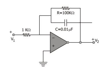
- The low frequency gain of the low pass filter shown in the given figure is
-
View Hint View Answer Discuss in Forum

V2 
= R . 1 V1 R1 RCs + 1 = 100 1 ≈ 100 10-3 j + 1 ∴ 20 log V2 = 40 dB V1 Correct Option: D
V2 = R . 1 V1 R1 RCs + 1 = 100 1 ≈ 100 10-3 j + 1 ∴ 20 log V2 = 40 dB V1
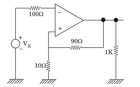
- Feedback factor for the circuit shown in the given figure is
-
View Hint View Answer Discuss in Forum
Feed back factor = 10 = 1 1000 100 Correct Option: D
Feed back factor = 10 = 1 1000 100
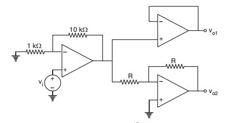
- For the circuit shown in figure, true relation is
-
View Hint View Answer Discuss in Forum
At second stage input to both op-amp circuit is same. Upper op-amp circuit is buffer having gain, AV = 1. Lower op-amp circuit is inverting amplifier having gain
Aυ = - R = - 1 R
∴ υ01 = – υ02Correct Option: B
At second stage input to both op-amp circuit is same. Upper op-amp circuit is buffer having gain, AV = 1. Lower op-amp circuit is inverting amplifier having gain
Aυ = - R = - 1 R
∴ υ01 = – υ02

