Analog electronics circuits miscellaneous
- The amplifier shown below is being used to amplify an input signal to a peak output voltage of 100 mV. What is the maximum operating frequency of the amplifier. Given slew rate is 0.5 V/µs
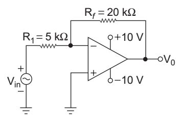
-
View Hint View Answer Discuss in Forum
fmax = Slew rate 2πVm = 0.5 × 106 = 796 kHz 2 × 3.14 × 100 × 10–3 Correct Option: B
fmax = Slew rate 2πVm = 0.5 × 106 = 796 kHz 2 × 3.14 × 100 × 10–3
- An op-amp has a CMRR of 90 dB. If its differential voltage gain is 30,000.Then its common mode gain is:
-
View Hint View Answer Discuss in Forum
CMRR = 20 log10 
Ad 
Ac 90 = 20 log10 30,000 Ac 4.5 = log10 30,000 Ac
or Ac = 30‚000 = 30‚000 = 0.9459 = 0.95 104.5 31622.77 Correct Option: B
CMRR = 20 log10 Ad Ac 90 = 20 log10 30,000 Ac 4.5 = log10 30,000 Ac
or Ac = 30‚000 = 30‚000 = 0.9459 = 0.95 104.5 31622.77
- A common-mode rejection ratio CMRR of an-amp, that has a differential gain of 2,00,000 and a common mode gain 6.33:
-
View Hint View Answer Discuss in Forum
CMRR in dB= 20 log10 Ad Ac = 20 log10 2‚00‚000 6·33
= 89.99
= 90 dBCorrect Option: A
CMRR in dB= 20 log10 Ad Ac = 20 log10 2‚00‚000 6·33
= 89.99
= 90 dB
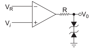
- In the OP amp. circuit with Zener diodes connected as shown, where the Zener voltage is VZ. V1 is the input signal and VR a reference voltage. The output Vo is given thus:
-
View Hint View Answer Discuss in Forum
NA
Correct Option: A
NA
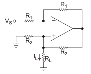
- In the op-amp circuit given below the load current iL is
-
View Hint View Answer Discuss in Forum
VA = VB (due to virtual ground)
KCL at node BVβ + VB – Vo + iL = 0 .............(i) R2 R2
KCL at node AVA – Vs + VA – Vo = 0 .............(ii) R1 R1 VA = Vs · R1 + Vo · R1 R1 + R1 R1 + R1 VA = Vs + Vo = VB 2 2 Vs + Vo Vs + Vo – Vo = 2 + 2 = – io R2 R2 Vs = – io R2 – io = Vs R2 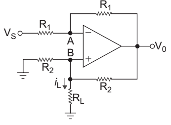
Correct Option: A
VA = VB (due to virtual ground)
KCL at node BVβ + VB – Vo + iL = 0 .............(i) R2 R2
KCL at node AVA – Vs + VA – Vo = 0 .............(ii) R1 R1 VA = Vs · R1 + Vo · R1 R1 + R1 R1 + R1 VA = Vs + Vo = VB 2 2 Vs + Vo Vs + Vo – Vo = 2 + 2 = – io R2 R2 Vs = – io R2 – io = Vs R2 

