-
What memory address range is NOT represented by chip #1 and chip #2 in the figure. A0 to A15 in this figure are the address lines and CS means chip select?

-
- 0100-02 FF
- F 900-FAFF
- 1500-16FF
- F800-F9FF
Correct Option: D
The given chip arrangement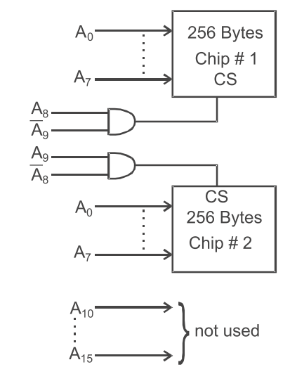
Given that CHIP Select (CS) is active high.
From figure we conclude that For chip #1 → A8 should be 1 and A9 should be 0 in order to make the chip select enable active.
For chip #2 → A8 should be 0 and A9 should be 1 in order to make the chip select enable active.
Given A10 – A15 not used it, we can use these bits either 0 or 1.
Now, this problem is further solved by applying Hit and Trial method
Add. lines: A15 A14 A13A12 A11 A10A9 A8 A7 A6 A5A4 A3 A2 A1 A0
Chip #1: X X X X X X 0 1 X X X X X X X X
Chip #2: X X X X X X 1 0 X X X X X X X X
Option (A) → 0100: for Chip #1 is possible
[0000 0001 0000 0000]
02FF: for Chip #2 is possible
[0000 0010 1111 1111]
Option (B) → F900: for Chip #1 is possible
[1111 1001 0000 0000]
FAFF: for Chip #2 is possible
[1111 1010 1111 1111]
Option (C) → 1500: for Chip #1 is possible
[0001 0101 0000 0000]
16FF: for Chip #2 is possible
[0001 0110 1111 1111]
Option (D) → F800: for Chip #1 is not possible
&nsbp;&nsbp;F9FF: for Chip #2 is not possible]
Hence alternative (D) is correct choice.

