-
A state diagram of a logic gate which exhibits a delay in the output is shown in the figure, where X is the don’t care condition, and Q is the output representing the state.
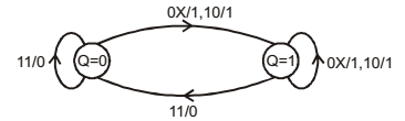
The logic gate represented by the state diagram is
-
- XOR
- OR
- AND
- NAND
Correct Option: D

If you will observe this true table corresponding to state diagram, then if any input is 0 output is 1 and if all the inputs are one output is zero it means it corresponds to NAND gate.

